







Sink/Source DDR Termination Regulator, EUP7998 Replace NCP51200.
EUP7998 EUP7998.pdf
EUP7998.pdfFEATURES
? VLDOIN Input Voltage Range: 1.1V to 3.5V
? VIN Input Voltage Range: 2.375V to 5.5V
? Typically 3×10μF MLCCs stable for DDR
? Fast Load-Transient Response
? ±10mA Buffered Reference (REFOUT)
? Meet DDR, DDR2 JEDEC Specifications.
Supports DDR3 and Low-Power DDR3/DDR4
VTT Applications
? Power-Good Window Comparator
? With Soft Start, UVLO and OCP
? Thermal Shutdown
? Available in 10-Pin 3mm×3mm TDFN and
SOP-8 (EP) packages
? RoHS Compliant and 100% Lead(Pb)-Free
Halogen-Free
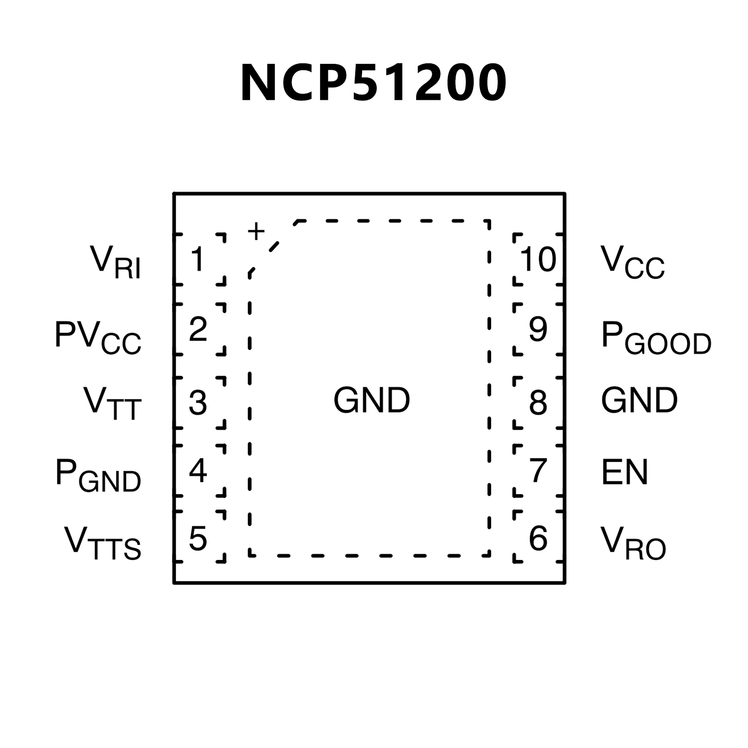
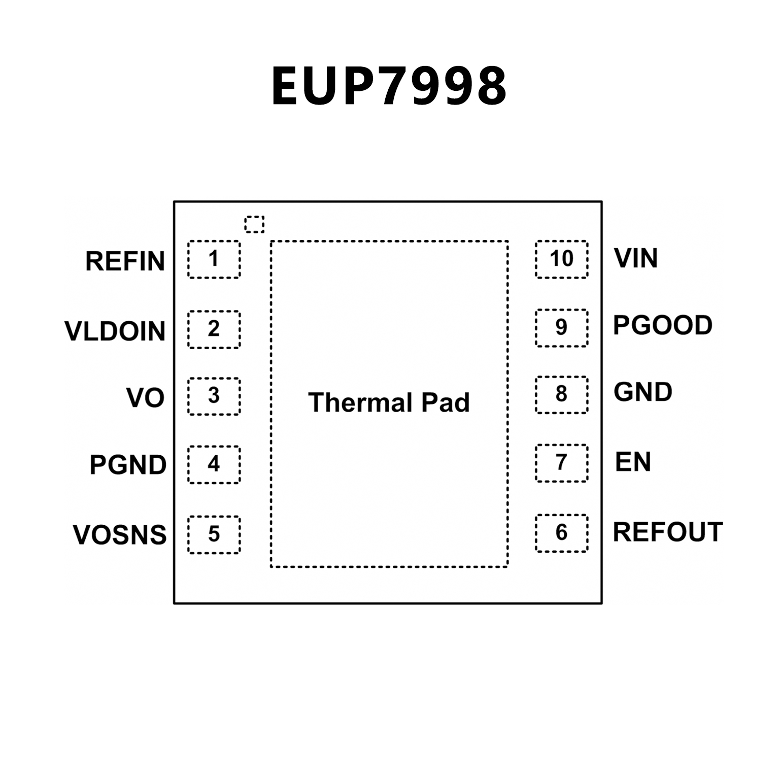
PIN CONFIGUTION
優(yōu)勢替代
FEATURES
? For Automotive Applications
? Input Voltage Rails: Supports 2.5 V, 3.3 V and 5 V Rails
? PVCC Voltage Range: 1.1 to 3.5 V
? Integrated Power MOSFETs
? Fast Load?Transient Response
? PGOOD ? Logic output pin to Monitor VTT Regulation
? EN ? Logic input pin for Shutdown mode
? VRI ? Reference Input Allows for Flexible Input Tracking
Either Directly or Through Resistor Divider
? Remote Sensing (VTTS)
? Built?in Soft Start, Under Voltage Lockout and Over
Current Limit
? Thermal Shutdown
? Small, Low?Profile 10?pin, 3x3 DFN Package
? NCV51200MWTXG (SFS), NCV51200MLTXG (SLP);
? Wettable Flank Options for Enhanced Optical Inspection
? NCV Prefix for Automotive and Other Applications
Requiring Unique Site and Control Change Requirements;
AEC?Q100 Qualified and PPAP Capable*
? These Devices are Pb?Free and are RoHS Compliant
PIN CONFIGUTION