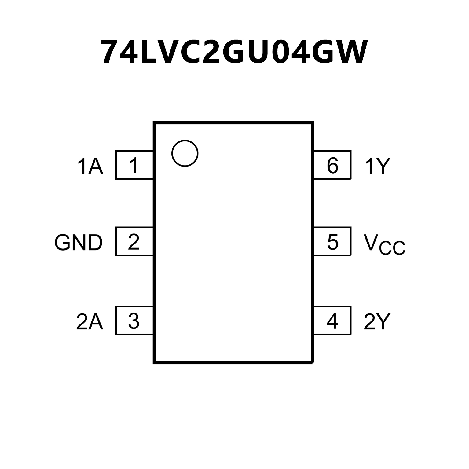








Dual unbuffered inverter, 74LVC2G04XC6G Replace 74LVC2GU04GW.
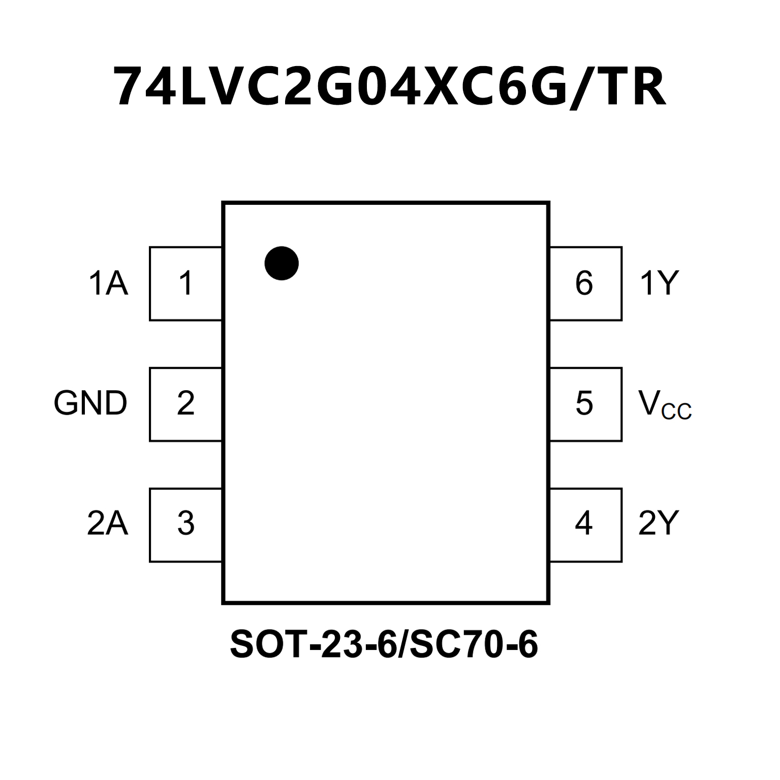
74LVC2G04XC6G/TR 74LVC2G04XC6G/TR.pdf
74LVC2G04XC6G/TR.pdfFEATURES
? 1.65V to 5.5V Wide Operating Voltage Range
? Input and Output Interface Capability to 5V
System Environment
? +24mA/-24mA Output Current at VCC = 3.0V
? CMOS Low Power Consumption
? Direct Interface with TTL Levels
? High Noise Immunity
? Latch-up Performance Exceeds 250mA
? -40℃ to +125℃ Operating Temperature Range
? Available in Green SOT-23-6 and SC70-6 Packages
PIN CONFIGUTION
優(yōu)勢(shì)替代
FEATURES
? Wide supply voltage range from 1.65V to 5.5V
? Overvoltage tolerant inputs to 5.5V
? High noise immunity
? ±24 mA output drive (VCC = 3.0V)
? CMOS low power dissipation
? Latch-up performance exceeds 250mA
? Complies with JEDEC standard no. 8-1A
? ESD protection:
? HBM: ANSI/ESDA/JEDEC JS-001 class 2 exceeds 2000V
? CDM: ANSI/ESDA/JEDEC JS-002 class C3 exceeds 1000V
? Multiple package options
? Specified from -40 °C to +85 °C and -40 °C to +125 °C
PIN CONFIGUTION